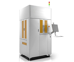
•The product meets the needs of semiconductor ultrasonic spraying photoresist technology. The unit module is designed around the Robot. It can be equipped with a variety of spray functional components to suitable for semiconductor high-end packaging/MEMS/optical modules/flexible substrates/irregular substrates and other different spraying photoresists process
•Suitable for 2, 4, 6, 8, 12 inch wafers ≤ 500mm and so on.
•Suitable for the substrate: silicon wafer, glass, ceramic, flexible film, metal, etc. It is suitable for the production of spraying process products with a film thickness of 0.8-20um.
 EN
EN 中文
中文